Activities
Laying out the PCB
Now select the 'PCB' tab, this will randomly place the components, and show a 'rats nest' of coloured lines indicating which pins need to be connected together.
The first thing we should do is fix the circuit board settings,
- select the grey rectangle background (this is the PCB)
- in the Inspector, set Layers: one layer (single-sided)
- now select each component and set PCB Layer: bottom
- As a guideline you will also need to set the size of your PCB to 45 x 35mm
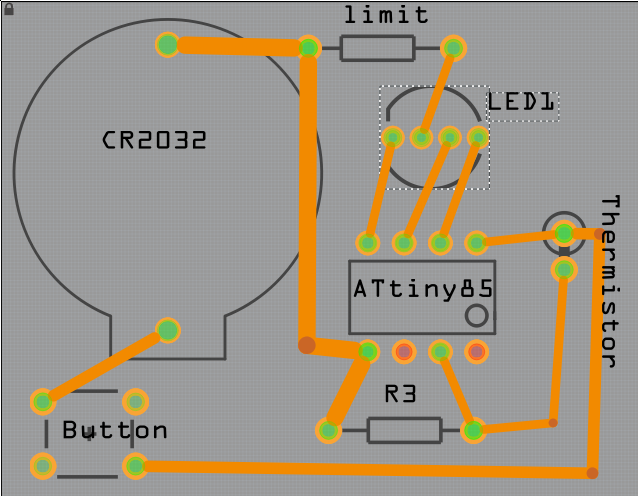
Rearrange the layout of your components, rotating them as necessary, until you can join the wires between them without any crossing over.
NB: We noticed a bug, although the LED pin ordering is set to RGB, and the attiny pins are also in this order, sometimes the rats nice falsely suggests that the green and blue wires cross, ignore this and connect them up as per the original connection listing.
Try to place the thermistor connection towards the right hand edge of the board, so that the component can be bent over the side of the board and protrude.
Select each wire and make them to at least Width: thick this makes the final circuit more robust and easier to solder.
Your completed circuit may look something like this...

Now you can export the completed circuit board into the 'Extended Gerber' format. Press the little triangle on the Export for PCB button and select the format.
Next Stage: Isolation Routing with FlatCAD

